Categories
- News (124)
- case study (6)
Recent News & Blog
 Why Museums Are Turning to Fine Pitch LED Displays for Better Visitor Engagement
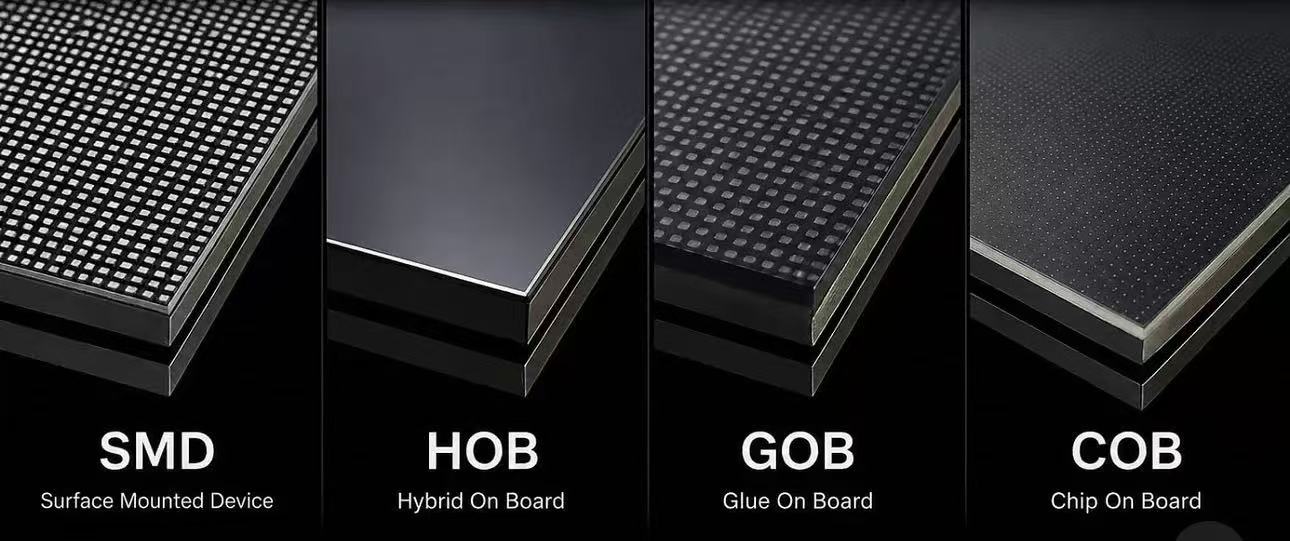
Structure: This is the most traditional and widely used technology. Individual LED packages (containing the red, green, and blue chips) are soldered directly onto the surface of the PCB (Printed Circuit Board).
Protection: Low. The diodes are exposed directly to the air, making them vulnerable to physical impact, moisture, and dust.
Pixel Pitch: Typically optimal for pixel pitches down to 1.2mm. Going smaller increases the risk of individual diodes breaking off.
Pros: Highly mature technology, cost-effective, excellent color uniformity, and very easy to repair (individual LEDs can be desoldered and replaced).
Cons: Fragile; LEDs can easily be knocked off during installation or cleaning.
Structure: HOB is an evolutionary upgrade to standard SMD. After the SMD LEDs are soldered onto the PCB, a thin, targeted layer of protective transparent glue is applied specifically around the base or over the diodes.
Protection: Moderate. It provides enhanced mechanical strength to prevent individual LEDs from being knocked off and offers basic moisture resistance.
Pros: Improves the physical durability of standard SMD screens without significantly increasing production costs or altering the visual properties of the display.
Cons: Does not offer a completely seamless, flat surface like GOB or COB, and protection against fine dust or heavy moisture is limited compared to full encapsulation.
Structure: GOB is an advanced protection technology for SMD modules. The standard SMD LEDs are soldered to the PCB, and then the entire module face is cast with an ultra-transparent epoxy or silicone glue, completely encapsulating the LEDs.
Protection: High (IP65-level face protection). It is waterproof, dustproof, anti-collision, anti-static, and UV-proof.
Pros: Creates a smooth, matte, or glossy surface that is highly durable and easy to wipe clean. It drastically reduces “dead light” rates caused by physical damage during transit or installation.
Cons: Harder to repair than standard SMD. If a diode fails underneath the glue layer, the glue must be precisely scraped away to fix it and then reapplied, which can sometimes leave visual blemishes.
Structure: COB is a fundamental shift in packaging technology. Instead of using packaged SMD LED diodes, the bare micro-LED chips (red, green, and blue) are bonded directly onto the PCB substrate. The entire module is then encapsulated with a transparent resin layer.
Protection: Highest. Because there are no exposed brackets or solder pins, it is exceptionally robust against physical impact, moisture, and dust.
Pixel Pitch: Ideal for Ultra-Fine Pixel Pitch (typically below 1.5mm down to 0.4mm).
Pros: Offers a completely flat, seamless surface with a wider viewing angle, higher contrast, reduced moiré effect, and better heat dissipation. It provides a more comfortable, paper-like viewing experience at close distances.
Cons: Highest cost; color uniformity can be difficult to calibrate across different production batches; individual pixel repair is highly complex and usually requires specialized factory equipment.
| Feature | SMD | HOB | GOB | COB |
| LED Packaging | Packaged Diodes | Packaged Diodes | Packaged Diodes | Bare Micro Chips |
| Surface Finish | Rough/Exposed | Semi-exposed | Completely Flat (Glue Layer) | Completely Flat (Resin Layer) |
| Impact Resistance | Low | Medium | High | Very High |
| Water/Dust Proof | Low | Low-Medium | High (IP65 Face) | High |
| Best Pixel Pitch | > 1.2mm | > 1.2mm | 0.9mm – 2.5mm | < 1.5mm (Ultra-fine) |
| Repairability | Very Easy | Moderate | Difficult | Very Difficult (Factory) |
| Relative Cost | Low | Low-Medium | Medium | High |
Why Museums Are Turning to Fine Pitch LED Displays for Better Visitor Engagement

 Sales Manager